Circuit laboratory / Five studies
The circuit, the reasoning and the evidence.
These studies cover analogue signal processing, mixed-signal logic and switching power. Each separates the intended behaviour from what the available schematic or diagram actually demonstrates.
Design values are not measured results. Where plots, simulation files or physical tests are not shown, this page does not claim verified performance.
01 / Active-inductor study
Antoniou GIC
An active circuit targeting the behaviour of a large grounded inductor. The study makes the ideal target and practical op-amp limits explicit.
Purpose
Explore how an active impedance-converter circuit can represent a large inductance without using a physical 10 H coil.
Design approach
The schematic combines two TL072 op-amps with a resistor-capacitor network. It specifies a 10 H ideal target and a 10 Hz–100 kHz AC sweep, using a test current source to examine the input impedance.
Evidence available
The available schematic records the topology, component values, supply rails and AC-analysis setup. Its annotation flags a model resonance; the response plot and native simulation files are not included in this case study.
What still needs checking
Compare simulated impedance magnitude and phase with the ideal inductive response, then identify the frequency range in which the model is a useful approximation.
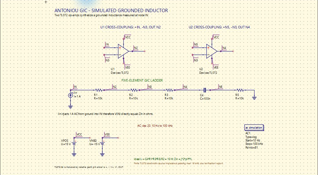
Scope and limitations: 10 H is a design target, not a measured inductance. The schematic alone does not establish a usable bandwidth, stability margin or agreement with hardware.
02 / Filter topology & debugging
KHN State-Variable Filter
A three-output filter study with a documented feedback-sign problem. The case study explains the intended response and why stability must be checked separately.
Purpose
Study a filter architecture that exposes high-pass, band-pass and low-pass outputs from a shared signal path.
Design approach
The drawing separates a summing stage from two integrators and labels the feedback paths. This makes it possible to follow how the output signals return to the summer and inspect their signs.
Evidence available
The schematic explicitly notes that its shown feedback sign gives negative damping. That issue is retained here as a debugging finding, not presented as a corrected or validated filter.
What still needs checking
Resolve the feedback-sign issue, then compare the intended transfer functions with both AC response and transient behaviour before making performance claims.
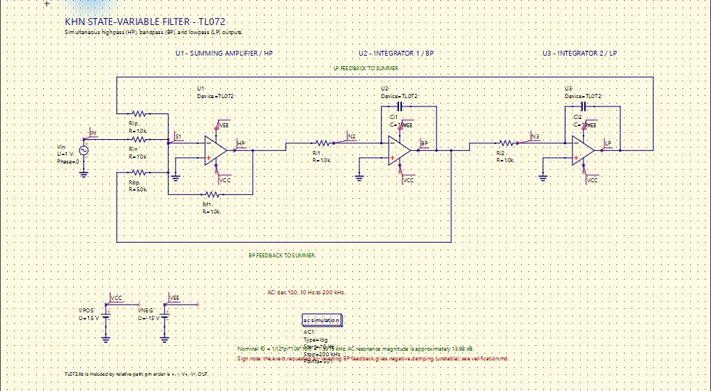
Scope and limitations: The shown design has a documented stability issue. A frequency-response setup is not proof of stable time-domain behaviour, and no corrected implementation is claimed here.
03 / Differential signal conditioning
Instrumentation Amplifier
A differential-amplifier study separating the input gain stage from the difference stage, with explicit component values and an AC test setup.
Purpose
Explore a signal-conditioning circuit intended to amplify the difference between two inputs rather than treating either input as the complete signal.
Design approach
Two TL072 stages form the input section and a third forms the difference amplifier. The drawing labels the gain-setting network, opposite-phase input sources and ±15 V supplies.
Evidence available
The schematic includes a 1 Hz–100 kHz AC sweep setup. It makes the two-stage architecture and resistor relationships inspectable, but does not provide measured noise, offset or common-mode rejection results.
What still needs checking
Check differential and common-mode gain separately, examine resistor-tolerance sensitivity, and verify operating range and clipping with an appropriate transient test.
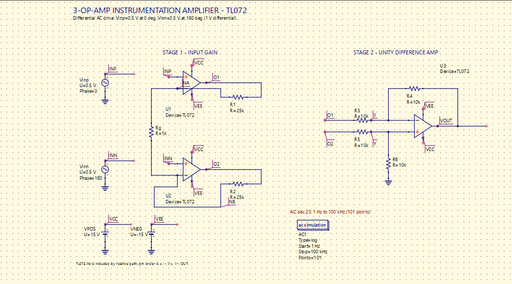
Scope and limitations: The configured small-signal AC analysis does not establish output headroom or large-signal behaviour. No precision, common-mode rejection or real sensor-interface performance is claimed.
04 / Mixed-signal concept
PFD + Charge Pump
A block-level study of how reference and feedback clock timing drives an analogue charge-pump output. The diagram separates the digital and analogue functions.
Purpose
Explain the interface between clock-comparison logic and the charge-pump output used as a building block in a phase-locked loop.
Design approach
The diagram groups reference and feedback clocks, two flip-flops with reset logic, and switched current sources labelled 100 μA. UP and DN labels connect the logic and analogue sections.
Evidence available
The available evidence is a concept diagram. It describes the functional blocks; it is not a transistor-level implementation, a simulation waveform or a complete phase-locked loop.
What still needs checking
Specify the clock and reset timing, exercise leading and lagging inputs in simulation, and evaluate charge-pump behaviour before connecting it to a complete loop.
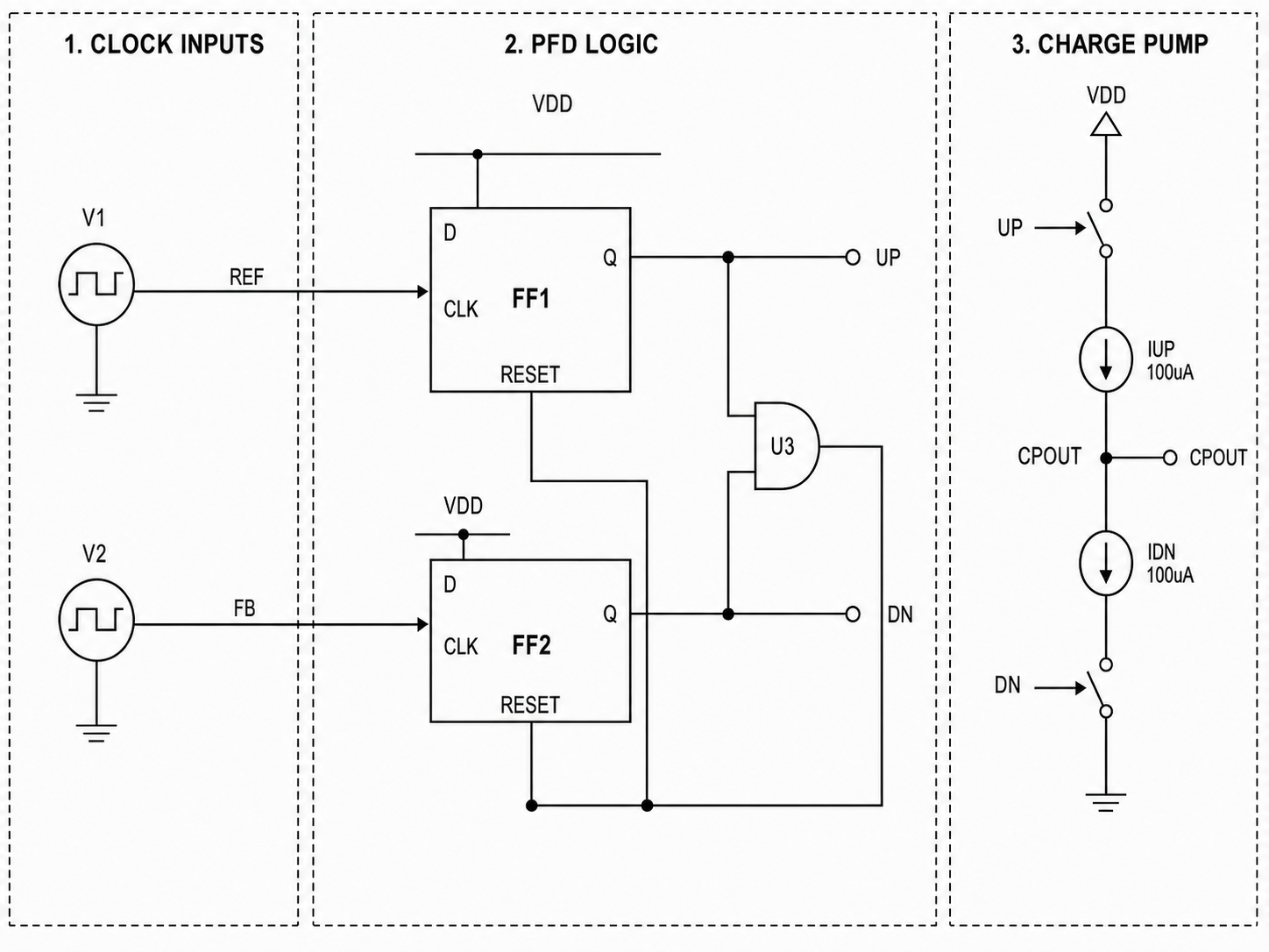
Scope and limitations: The nominal current labels do not establish current matching, dead-zone behaviour, jitter, output compliance or loop lock. Those results have not been demonstrated in this case study.
05 / Power-stage concept
Boost Converter
A step-up power-stage study showing the inductor, switch, rectifier and output network. It separates the proposed topology from unverified output performance.
Purpose
Study the elements of a switching power stage intended to produce an output voltage above its input.
Design approach
The diagram specifies a 12 V source, a 100 μH inductor, a controlled switch, a 1N5819 Schottky diode, a 100 μF capacitor and a 50 Ω load. A PWM source drives the switch; no feedback-regulation loop is shown.
Evidence available
The diagram identifies the power-stage components and connections. It does not include switching waveforms, a defined duty cycle or measured output results.
What still needs checking
Define switching conditions and device models, then evaluate startup, inductor current, output ripple and component ratings across the intended load range.
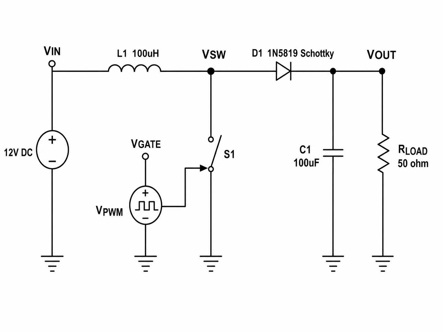
Scope and limitations: This is an open-loop concept, not a validated power supply. Output voltage, ripple, efficiency, component stresses and thermal limits remain unverified.