Hardware case study / KiCad 10 / Rev C
An organised interface between controller, sensors and relays.
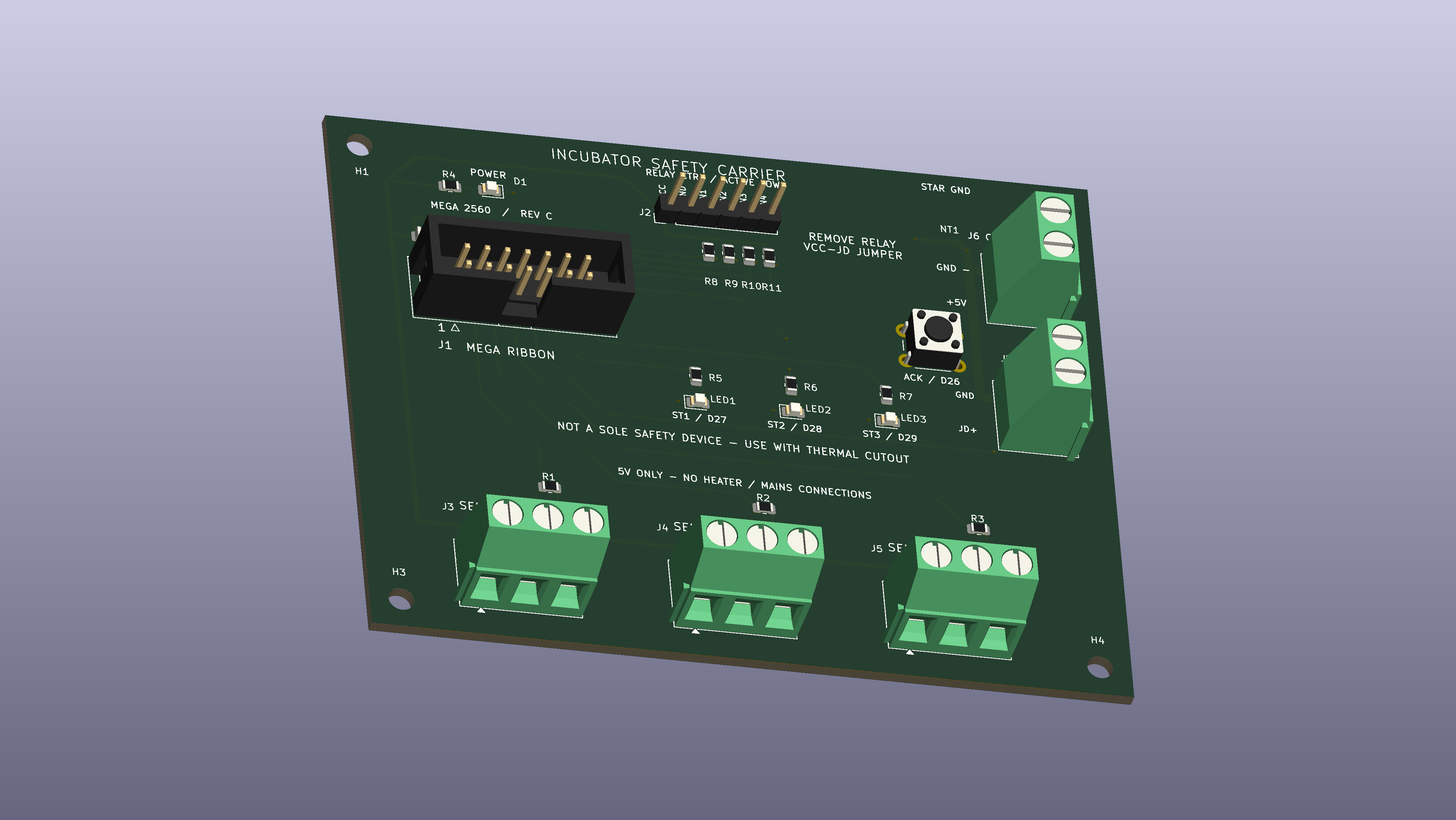
This carrier board brings the low-voltage connections for an Arduino Mega-based incubator controller onto a compact PCB. My PCB work focuses on component placement, routing, connector access and layout verification.
CAD design checked · not assembled or bench-tested- Board outline
- 96 × 76 mm
- Construction
- 2 copper layers
- Layout scope
- 30 footprints · 4 mounting holes
- Recorded review
- 12 September 2026
The design brief
Make the interface clear, accessible and checkable.
The board groups three temperature-sensor connections, four relay-control signals, status LEDs and an acknowledgement button. A keyed ribbon connector provides the controller interface; separate terminals handle the relay-coil supply. This is an interface carrier, not a complete incubator controller or a standalone safety system.
PCB decisions
Placement and routing with a reason behind them.
Connectors at the board edges
Sensor terminals sit along the lower edge; coil-supply terminals sit on the right. Placement leaves room for wiring and keeps the four mounting holes accessible.
Different routes for different jobs
Signal traces use a 0.30 mm width. The coil-positive route uses 1.50 mm and the main coil return uses 1.20 mm. These are design choices, not measured current-capacity guarantees.
A deliberate ground connection
The logic and coil ground regions meet at the NT1 copper net tie. The actual relay module must be checked for additional internal ground connections before the complete system can be validated.
Mechanical checks alongside electrical checks
The layout accounts for terminal-body setbacks, mounting-hole keepouts, courtyards and connector orientation. Physical fit still needs confirmation with the purchased parts.

Schematic organisation
Trace each interface before following the copper.
The schematic separates the controller header, three sensor interfaces, relay-control connections, coil-power path, indicators and acknowledgement button. This makes the relationship between the intended connections and the board easier to review.

Verification record
What was checked—and what those checks mean.
These results come from the saved KiCad 10.0.3 reports dated 12 September 2026. They are CAD checks, not physical test results.
- Schematic electrical-rule check (ERC)
- 0 errors and 0 warnings reported under the saved check configuration.
- PCB design-rule check (DRC)
- 0 violations and 0 unconnected pads reported under the saved check configuration.
- Schematic-to-PCB agreement
- The verification record reports 0 parity issues and 71 matching electrical pin assignments in a separate pin-map audit.
- Mechanical review
- Board outline, mounting-hole clearances and terminal-body positions documented. A 3D view checks model placement, not actual part fit.
The reports retain KiCad’s listed default ignored checks. A clean ERC/DRC result is not proof of functional performance, safe operation or certification.